SPICE is a circuit simulation tool written at the University of California Berkeley. It has been available to the public since the mid-1970s. It is considered the industry standard integrated circuit simulator. SPICE is an acronym for Simulation Program with Integrated Circuit Emphasis SPICE is mature and reliable software. Versions of SPICE are available for most operating systems. At MSOE, the PSPICE version is available through the Add/Remove programs feature of Microsoft Windows. For Macintosh users, the MacSPICE program is excellent software. Linux users will find precompiled packages of SPICE in most port collections.
The SPICE simulation engine accepts text file inputs. Most engineers refer to these text files as SPICE sourcecode, SPICE files, or SPICE decks. SPICE decks consist of cards organized into white-space separated fields. Cards may be one line of text or multiple lines of text. Each card of the SPICE deck contains an element description, a model definition, or a control statement. SPICE decks typically contain comments to help the engineer and other readers of the file. Today, many schematic CAD tools process schematic designs and automatically create the SPICE input deck for the user. Schematic entry is an attractive option for many circuit simulations. but is often not useful when the number of circuit elements grows exponentially large. This is true for many digital integrated circuits.
| TYPE DESIGNATOR | CIRCUIT ELEMENT |
| C | capacitor |
| E | voltage-controlled voltage source |
| F | current-controlled current source |
| G | voltage-controlled current source |
| H | current-controlled voltage source |
| I | independent current source |
| K | mutual-inductance coils |
| L | inductor |
| M | mosfet transistor |
| Q | bjt transistor |
| R | resistor |
| V | independent voltage source |
| SYMBOL | VALUE |
| T | 1E12 |
| G | 1E9 |
| MEG | 1E6 |
| K | 1E3 |
| M | 1E-3 |
| U | 1E-6 |
| N | 1E-9 |
| P | 1E-12 |
| F | 1E-15 |
| CIRCUIT TO BE ANALYZED |
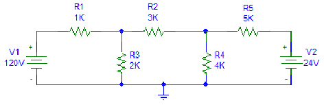 |
| SPICE INPUT DECK |
****************************************** * FILENAME: basicdc.cir * * AUTHOR: meier@msoe.edu <Russ Meier> * * DATE: 10 Apr 2002 * * PROVIDES: An example DC analysis * ****************************************** *********************************** * CIRCUIT DESCRIPTION * * card format: name nodes params * *********************************** V1 1 0 DC 120 R1 1 2 1K R3 2 0 2K R2 2 3 3K R4 3 0 4K R5 3 4 5K V2 4 0 DC 24V .END |
| SPICE OUTPUT |
NODE VOLTAGE NODE VOLTAGE NODE VOLTAGE NODE VOLTAGE ( 1) 120.0000 ( 2) 72.1510 ( 3) 36.8300 ( 4) 24.0000 VOLTAGE SOURCE CURRENTS NAME CURRENT V1 -4.785E-02 V2 2.566E-03 TOTAL POWER DISSIPATION 5.68E+00 WATTS JOB CONCLUDED |
| COMMENTS |
SPICE always performs a DC analysis on the circuit. Thus, no control statements are needed for basic DC analysis. Sweeps of DC voltage will require a control statement. |
| CIRCUIT TO BE ANALYZED |
|
| SPICE INPUT DECK |
****************************************** * FILENAME: basicdcsweep.cir * * AUTHOR: meier@msoe.edu <Russ Meier> * * DATE: 10 Apr 2002 * * PROVIDES: An example DC analysis * ****************************************** *********************************** * CIRCUIT DESCRIPTION * * card format: name nodes params * *********************************** V1 1 0 DC 120 R1 1 2 1K R3 2 0 2K R2 2 3 3K R4 3 0 4K R5 3 4 5K V2 4 0 DC 24V .DC LIN V2 0 24 2V .PRINT DC V(1) V(2) V(3) V(4) I(R5) .END |
| SPICE OUTPUT |
V2 V(1) V(2) V(3) V(4) I(R5) 0.000E+00 1.200E+02 7.094E+01 3.019E+01 0.000E+00 6.038E-03 2.000E+00 1.200E+02 7.104E+01 3.074E+01 2.000E+00 5.748E-03 4.000E+00 1.200E+02 7.114E+01 3.130E+01 4.000E+00 5.459E-03 6.000E+00 1.200E+02 7.125E+01 3.185E+01 6.000E+00 5.170E-03 8.000E+00 1.200E+02 7.135E+01 3.240E+01 8.000E+00 4.881E-03 1.000E+01 1.200E+02 7.145E+01 3.296E+01 1.000E+01 4.591E-03 1.200E+01 1.200E+02 7.155E+01 3.351E+01 1.200E+01 4.302E-03 1.400E+01 1.200E+02 7.165E+01 3.406E+01 1.400E+01 4.013E-03 1.600E+01 1.200E+02 7.175E+01 3.462E+01 1.600E+01 3.723E-03 1.800E+01 1.200E+02 7.185E+01 3.517E+01 1.800E+01 3.434E-03 2.000E+01 1.200E+02 7.195E+01 3.572E+01 2.000E+01 3.145E-03 2.200E+01 1.200E+02 7.205E+01 3.628E+01 2.200E+01 2.855E-03 2.400E+01 1.200E+02 7.215E+01 3.683E+01 2.400E+01 2.566E-03 JOB CONCLUDED |
| COMMENTS |
The DC sweep control statement sweeps a DC source through a range of values. A DC analysis is performed for each value. The sweep axis type is linear. A table is produced using the print control statement. |
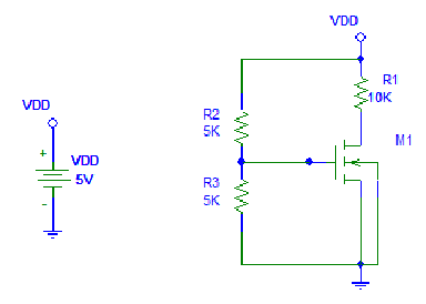
| CIRCUIT TO BE ANALYZED |
 |
| SPICE INPUT DECK |
****************************************** * FILENAME: basicdcq.cir * * AUTHOR: meier@msoe.edu <Russ Meier> * * DATE: 10 Apr 2002 * * PROVIDES: An example DC analysis * ****************************************** ******************************************** * MODEL DESCRIPTION * * card format: .model name type (params= ) * ******************************************** .model NMOD NMOS (LEVEL=1 VTO=1.5V KP=100U GAMMA=0 LAMBDA=0) *********************************** * CIRCUIT DESCRIPTION * * card format: name nodes params * *********************************** VDD 1 0 DC 5V R1 1 2 10K R2 1 3 5K R3 3 0 5K M1 2 3 0 0 NMOD L=2U W=2U .END |
| SPICE OUTPUT |
NODE VOLTAGE NODE VOLTAGE NODE VOLTAGE NODE VOLTAGE ( 1) 5.0000 ( 2) 4.5000 ( 3) 2.5000 VOLTAGE SOURCE CURRENTS NAME CURRENT VDD -5.500E-04 TOTAL POWER DISSIPATION 2.75E-03 WATTS JOB CONCLUDED |
| COMMENTS |
Semiconductor devices use model control statements to describe physical parameters. Level 1 MOS simulation is basically the general channel approximation model for MOSFET current. Level 1 is completely defined by five parameters: - PHI: the Fermi potential - GAMMA: the substrate-bias coefficient - LAMBDA: the channel-length modulation factor - VTO: the threshold voltage with zero substrate bias - KP: the conduction parameter k' = un * Cox Parameters not specified have default values. References exist for parameters and defaults. The MOSFET element card format is: name node-drain node-gate node-source node-substrate params MOSFET parameters specified in the element card are instance-parameters overriding model params. |
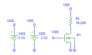
| CIRCUIT TO BE ANALYZED |
 |
| SPICE INPUT DECK |
************************************************************************** * FILENAME: RLIAPR11.cir * * AUTHOR: meier@msoe.edu <Russ Meier> * * DATE: 11 Apr 2002 * * PROVIDES: the RLI inverter from 11 Apr 2002 EE393 LECTURE * ************************************************************************** ********** * MODELS * ********** .model NMOD NMOS (LEVEL=1 VTO = 0.8V KP = 75U GAMMA = 0 LAMBDA = 0) *********************** * CIRCUIT DESCRIPTION * *********************** VDD 3 0 DC 3.3 VGS 1 0 DC 3.3 R1 2 3 19.200K M1 2 1 0 0 NMOD L=8U W=72.5640U ********************** * CONTROL STATEMENTS * ********************** .OP .DC LIN VGS 0 3.3 0.1 .PLOT DC V(2) .PROBE .END |
| SPICE OUTPUT |
************************************************************************* **** DC TRANSFER CURVES TEMPERATURE = 27.000 DEG C ****************************************************************************** VGS V(2) 0.0000E+00 1.0000E+00 2.0000E+00 3.0000E+00 4.0000E+00 _ _ _ _ _ _ _ _ _ _ _ _ _ _ _ _ _ _ _ _ _ _ _ _ _ _ _ 0.000E+00 3.300E+00 . . . . * . 1.000E-01 3.300E+00 . . . . * . 2.000E-01 3.300E+00 . . . . * . 3.000E-01 3.300E+00 . . . . * . 4.000E-01 3.300E+00 . . . . * . 5.000E-01 3.300E+00 . . . . * . 6.000E-01 3.300E+00 . . . . * . 7.000E-01 3.300E+00 . . . . * . 8.000E-01 3.300E+00 . . . . * . 9.000E-01 3.235E+00 . . . . * . 1.000E+00 3.039E+00 . . . .* . 1.100E+00 2.712E+00 . . . * . . 1.200E+00 2.255E+00 . . . * . . 1.300E+00 1.667E+00 . . * . . . 1.400E+00 9.489E-01 . *. . . . 1.500E+00 4.639E-01 . * . . . . 1.600E+00 3.637E-01 . * . . . . 1.700E+00 3.070E-01 . * . . . . 1.800E+00 2.681E-01 . * . . . . 1.900E+00 2.390E-01 . * . . . . 2.000E+00 2.162E-01 . * . . . . 2.100E+00 1.977E-01 . * . . . . 2.200E+00 1.824E-01 . * . . . . 2.300E+00 1.694E-01 . * . . . . 2.400E+00 1.582E-01 . * . . . . 2.500E+00 1.484E-01 . * . . . . 2.600E+00 1.398E-01 . * . . . . 2.700E+00 1.322E-01 . * . . . . 2.800E+00 1.255E-01 . * . . . . 2.900E+00 1.194E-01 . * . . . . 3.000E+00 1.138E-01 .* . . . . 3.100E+00 1.088E-01 .* . . . . 3.200E+00 1.042E-01 .* . . . . 3.300E+00 1.000E-01 .* . . . . - - - - - - - - - - - - - - - - - - - - - - - - - - - **** 04/11/02 11:24:29 *********** Evaluation PSpice (Nov 1999) ************** ************************************************************************** **** SMALL SIGNAL BIAS SOLUTION TEMPERATURE = 27.000 DEG C ****************************************************************************** NODE VOLTAGE NODE VOLTAGE NODE VOLTAGE NODE VOLTAGE ( 1) 3.3000 ( 2) .1000 ( 3) 3.3000 VOLTAGE SOURCE CURRENTS NAME CURRENT VDD -1.667E-04 VGS 0.000E+00 TOTAL POWER DISSIPATION 5.50E-04 WATTS |
| COMMENTS |
This example sweeps the input voltage, VGS, using the .DC control statement. This produces the voltage-transfer characteristic VDS versus VGS. The .PLOT control statement prints the tabular values and creates an ASCII plot for voltage V(2). The operating point (DC circuit analysis: non-sweep) is requested with the .OP control statement. It would not be provided in the absence of .OP because SPICE is DC sweeping VGS. This provides the high input / low output power information. Note that the current is correct. Current out of a source positive terminal is a negative current in circuit theory. The .PROBE control statement records analysis data for use by the Probe waveform viewer. |
| CIRCUIT TO BE ANALYZED |
|
| SPICE INPUT DECK |
**************************************************************************
* FILENAME: apr11.cir                                                    *
* AUTHOR: meier@msoe.edu <Russ Meier>                                    *
* DATE: 11 Apr 2002                                                      *
* PROVIDES: the RLI inverter from 11 Apr 2002                            *
**************************************************************************

**********
* MODELS *
**********

.model NMOD NMOS (LEVEL=1 VTO = 1.5V KP = 150U GAMMA = 0 LAMBDA = 0)

*************
* PARAMTERS *
*************

.param RL=10K

***********************
* CIRCUIT DESCRIPTION *
***********************

VDD 3 0 DC 5
VGS 1 0 DC 5
R1 2 3 {RL}
M1 2 1 0 0 NMOD L=10U W=10U

**********************
* CONTROL STATEMENTS *
**********************
.OP
.STEP LIN PARAM=RL 10K 50K 10K
.DC LIN VGS 0 5 0.1
.PLOT DC V(2)
.PROBE
.END
|
| SPICE OUTPUT |
TRY IT! Probe output is: |
| COMMENTS |
This example steps the parameter RL through a linear range of values. The starting value is 10K, the final value is 50K, and the resolution is 10K SPICE runs the requested commands (.DC and .PLOT) for each of the parameter steps. I do not remember the history of the .PARAM and .STEP commands. I believe the .PARAM and .STEP commands were introduced by PSpice. Berkeley SPICE has the .ALTER command to do multiple runs for changing parameters. Probe is also a PSpice addition. The Berkeley SPICE waveform plotter is called nutmeg. |
| CIRCUIT TO BE ANALYZED |
| CMOS INVERTER |
| SPICE INPUT DECK |
INVERTER TRANSIENT ANALYSIS ********** * MODELS * ********** .model NMOD NMOS (LEVEL=1, VTO=0.7 GAMMA=0 LAMBDA=0 KP=73U) .model PMOD PMOS (LEVEL=1, VTO=-0.8 GAMMA=0 LAMBDA=0 KP=21U) *********** * CIRCUIT * *********** VDD 3 0 DC 5 VGS 1 0 PULSE(0,5,0,5n,5n,1u,2u) M1 2 1 0 0 NMOD L=2U W=10U M2 2 1 3 3 PMOD L=2U W=25U C1 2 0 0.047n .OP .TRAN 0.1U 3U .PLOT TRAN V(2) .PROBE .END |
| SPICE OUTPUT |
TRY IT! Probe output is: |
| COMMENTS |
This example uses a pulse input voltage model. The pulse parameters are separated by commas. The parameters in order are: initial voltage V1, pulsed voltage value V2, delay time TD, rise time TR, fall time TF, pulse width PW, and period PER. The transient control statement syntax is: .tran step stop optional:start optional:max A capacitor was added to simulate load capacitance. |
This page was last modified on
These information pages are copyright © Russ Meier. All rights
reserved.
