WEEK 2 LEARNING OBJECTIVES
Day 1
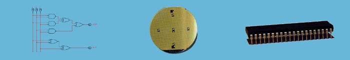
- List the four basic steps in wafer
fabrication.
- Describe the process of oxide growth and
- Describe the purpose of oxide growth.
- Describe the process of ion implantation
- Describe the purpose of ion implantation.
- Describe the process of etching.
- Describe the purpose of etching.
Day 2
- Describe the process of photo-resist.
- Describe the purpose of photo-resist.
- List the "layers" of material that are
typically seen in a CMOS electronic device.
- Describe the resist-expose-solvent-etch
procedure.