Each pair of students will also need two banana to banana patch cords (one red and one black) from the rack on the wall in the lab.
Dangerous line voltages are present at the outlets on your work bench. Do not insert anything other than approved power plugs into these outlets.
The voltages and currents produced by the Digi Designer are generally safe. However, you should not short +5V (Vcc) or logic High outputs directly to ground or intentionally make yourself part of a logic circuit.
The DC power supplies can produce dangerous voltages and current if the voltage knob is turned too far in the clockwise direction. Keep the power supplies on the 15 volt range and do not turn the voltage knob past the point where the output voltage reaches 5.5 volts.
Chip pins and the tips of the small wires may be sharp. Handle with care. Chips can become very hot if wired incorrectly. Be careful.
Identify the equipment you will be using based on the following figures. Glance over these figures now and refer back to them as needed as you go through the rest of the procedures.
|
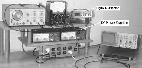
| Figure 1 -- A typical work station in S-314 with the digital multimeter (DMM) and DC power supplies identified. |
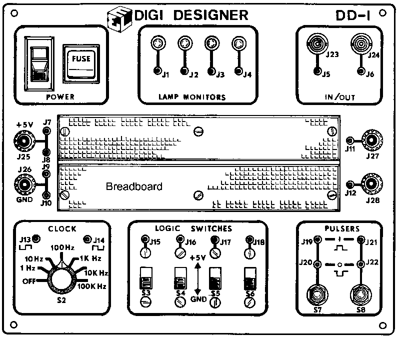 |
| Figure 2 -- The front panel of a Digi Designer. |
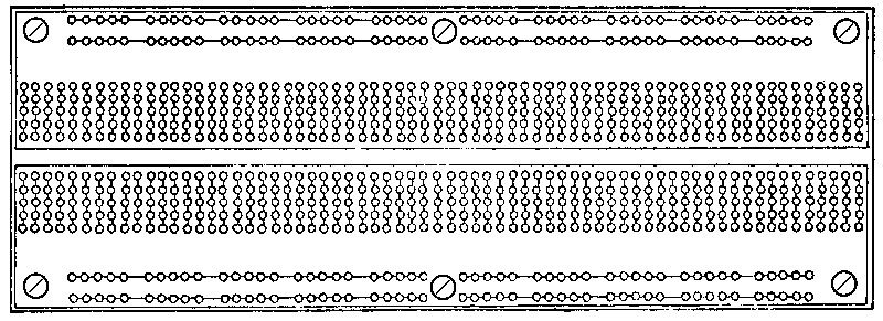 |
| Figure 3 -- Connections between the various rows and columns of holes on a standard bread board. |
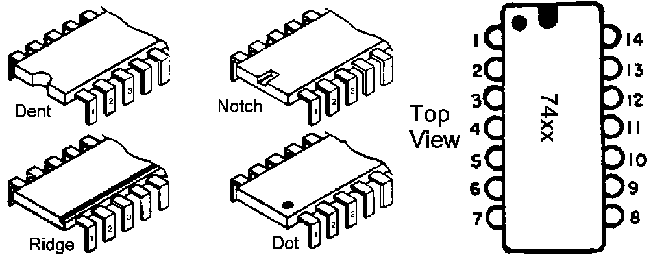 |
| Figure 4 -- How to identify pin 1 on various designs of Dual In-Line Package (DIP) chips and how the pins are numbered starting with pin 1 and preceding counter-clockwise around the chip. |
 |
| Figure 5 -- How to orient a chip on the bread board and make connections to it. |
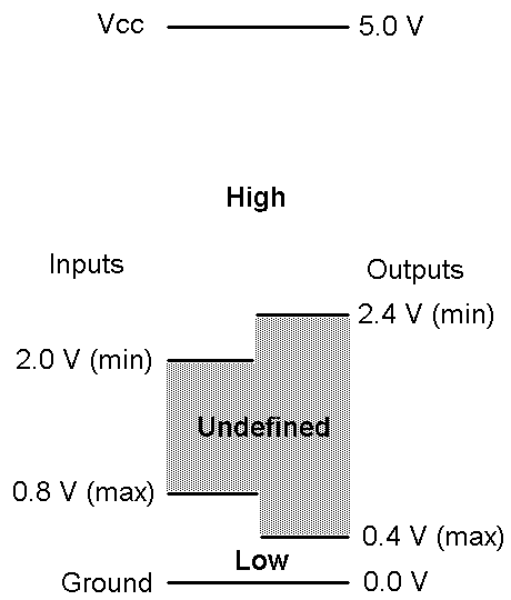 |
| Figure 6 -- This figure shows the TTL level specifications for logic High and Low. Also shown are the normal values for Vcc and ground. |
Plug in and switch on the Digi Designer. As long as you don't create any shorts between Vcc (+5V) and ground (GND) you can leave it on throughout the experiments. Turn on the digital multimeter (DMM) shown in Figure 1. Be sure that the black DMM lead is connected to the Common socket on the DMM and the red DMM lead to the V/K{Omega}/S socket on the DMM. Select the DC mode, the V (volts) mode and the 20 range on the DMM.
You will now check to see if the +V5 output connector on the Digi Designer really provides about 5 volts. Use an alligator clip patch cord to connect the black DMM lead to the black GND (ground) connector on the Digi Designer. Use another alligator clip patch cord to connect the red +5V (Vcc) connector on the Digi Designer. Read and record the voltage displayed on the DMM. It should be about 5 volts. Is it? If not, double check your set up.
Next, you will check to see if the unloaded push buttons really produce logic Low (usually considered 0 or False) and logic High (usually considered 1 or True) outputs. Move the alligator clip from the +5V connector to the upper left pulser output connector (the one labeled J19 in Figure 2). Read the pulser Low voltage and compare your result with Figure 6. Is the pulser Low voltage within the TTL Low output range? If not, double check your set up.
Press and hold the left pulser button (the one labeled S7 in Figure 2) and record the pulser High output voltage. Is the pulser High voltage within the TTL High output range? If not, double check your set up.
Now you will determine if a load changes the pulser output voltages. Leave the DMM connected to the pulser output and run a wire from the pulser output connector to one of the Lamp Monitors. Repeat the pulser Low and High output measurements described previously. Did the voltages change? Are they still within the specified TLL ranges? I would expect the voltages to change due to the finite internal resistance of the the pulser outputs.
Next, you'll check the LED monitor lamps to see if they respond as you would expect to input voltages. Move the alligator clip from the pulser output connector to one of the Lamp Monitor (LED) connectors (J1, J2, J3 or J4 in Figure 2). Switch one of the DC power supplies (shown in Figure 1) to the 15 V range, turn its V (voltage) knob fully counter-clockwise, its C (current) knob fully clockwise and switch it on. Use a black banana to banana patch cord to connect the black (-) terminal on the power supply to the black (GND) terminal on the Digi Designer. Use a red banana to banana patch cord to connect the red (+) terminal on the power supply to the upper (white) connector on the right side of the Digi Designer front panel (J27 in Figure 2) Note, do not connect the red (+) power supply terminal to the red (+5V) Digi Designer terminal. Next, run a wire from J11 to the LED connector you have the red DMM lead connected to. Read and record the voltage at LED (and J11 via the wire). Without exceeding 5.5 volts, slowly turn up the power supply output voltage by turning it V knob clockwise. Watch the LED. Complete the table given in the work sheet. Use terms like Off, Dim and Bright in the table to describe the LED response. Is the LED response consistent with the TTL input voltage ranges given in Figure 6? Switch off the power supply and DMM. Disconnect them from the Digi Designer.
 |
 |
 |
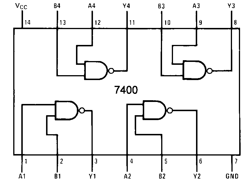 |
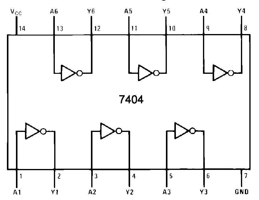
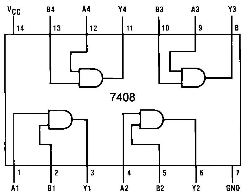
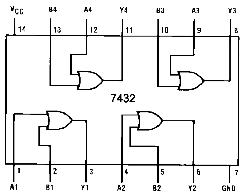
| Figure 7 -- Pin outs for the 7404 hex inverter, 7408 quad AND, 7432 quad OR and 7400 quad NAND chips. | |
Plug your 7404 chip into the bread board on your Digi Designer. Orient the chip like the 7400 shown in Figure 5. Connect connect pin 7 of the chip to ground (GND) and connect pin 14 of the chip to power (+5V). Connect the output from one of the pulsers to pin 1 on the chip. Also run a wire from pin 1 to an LED. This LED will display the pulser output/inverter input. Connect the inverter output from the chip's pin 2 to a different LED. This LED will display the inverter output. Press the push button and watch the LED's. Complete the table given on the work sheet. Are these the results you expected? If not, double check your wiring.
Replace the 7404 with your 7408. Connect a wire from the unused pulser to pin 2 on the 7408. Connect the output of the AND gate (pin 3) to an LED. Press the buttons in order to complete the table given in the work sheet. Did you obtain the expected results? If not, double check your wiring.
Replace the 7408 with your 7432. Press the buttons in order to complete the table given in the work sheet. Did you obtain the expected results? If not, double check your wiring.
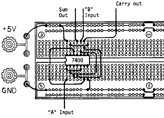
Replace the 7432 with your 7400. Press the buttons in order to complete the table given in the work sheet. Did you obtain the expected results? If not, double check your wiring.
L = (T + H)F + (T + H)'B
In ordinary English this means that the tail light, L, should flash when the turn signal or hazard switch is on or if neither the signal or hazard switch is on then pressing the brake pedal should cause the tail light to come on.
Figure 8 shows the logic diagram that corresponds to the equation given above. Figure 9 shows a wiring diagram for implementing the equation using one 7404, one 7408 and one 7432.
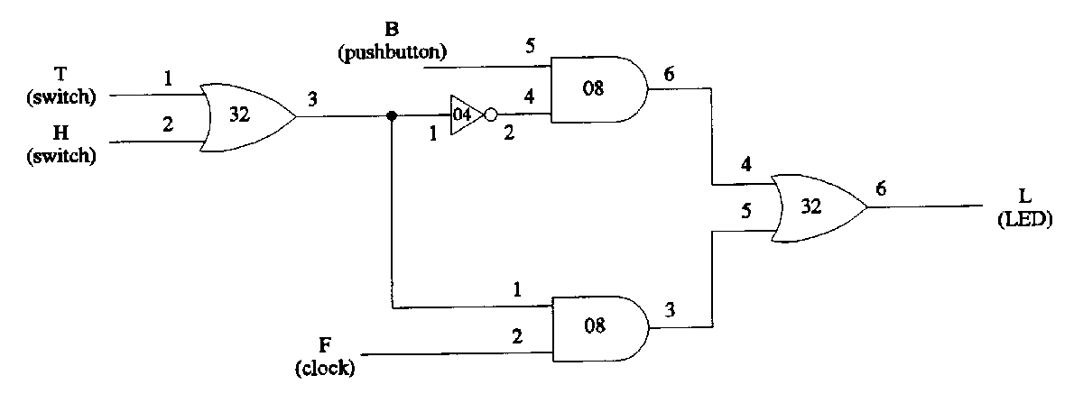 |
| Figure 8 -- Tail light logic diagram. |
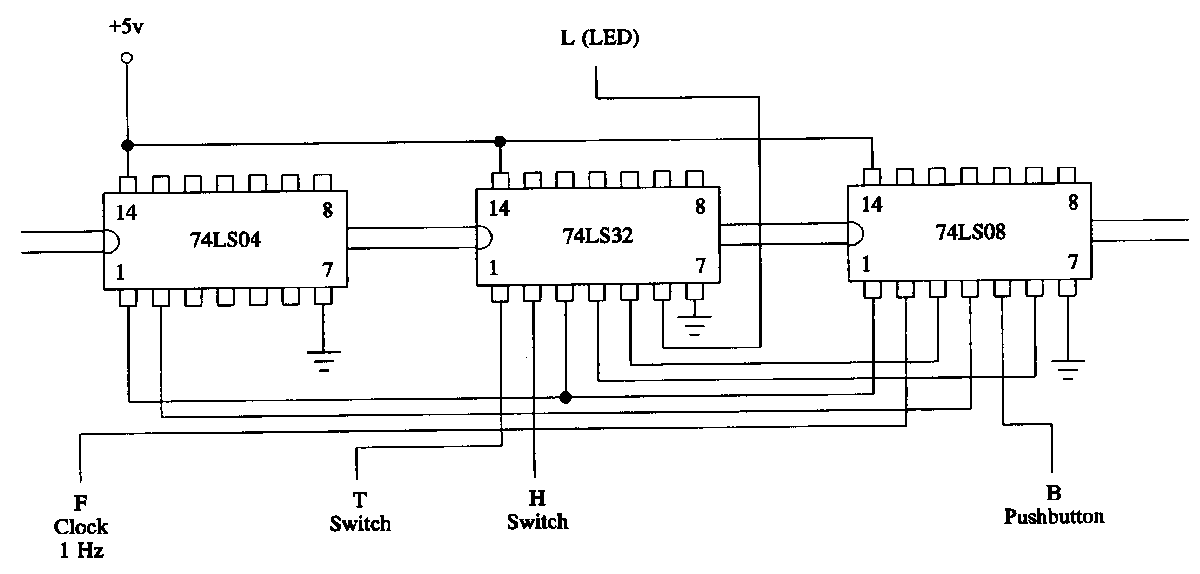 |
| Figure 9 -- Tail light wiring diagram. |
Build the circuit shown in Figure 9 on your Digi Designer. Test your circuit and record your results on your work sheet. Use the terms On, Off and Flashing to describe the tail light status. If your circuit does not work initially, try debugging (fixing) it by systematically eliminating possible problems. This example was suggested by MSOE faculty member Dr. Henry Welch.
The Digi Designer illustrations in this document were taken from the Digi Designer manual and the chip pin out diagrams were taken from Fairchild/National Instruments chip data sheets.