Memory makes up a very important part of digital computers. One type of memory is Erasable, Programmable Read Only Memory (EPROM). You will retrieve an ASCII message stored in an 2732 EPROM chip in this exercise.
Dangerous line voltages are present at the outlets on your work bench. Do not inert anything other than approved power plugs into these outlets.
The voltages and currents produced by the Digi Designer are generally safe. However, you should not short +5V (Vcc) or logic High outputs directly to ground or intentionally make yourself part of a logic circuit.
Chip pins and the tips of the small wires may be sharp. Handle with care. Chips can become very hot if wired incorrectly. Be careful.
|
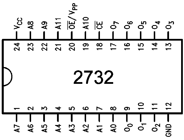
| Figure 1 -- Pin outs for the 2732 EPROM chip. |
Insert your 2732 into the bread board on your Digi Designer. Connect power and ground to pins 24 and 12, respectively. Make the following connections from left to right across the lower edge of the chip:
| Pin | Function | Connection |
|---|---|---|
| 1 | A7 input | Ground, logic Zero |
| 2 | A6 input | Ground, logic Zero |
| 3 | A5 input | Ground, logic Zero |
| 4 | A4 input | Ground, logic Zero |
| 5 | A3 input | J15, switch |
| 6 | A2 input | J16, switch |
| 7 | A1 input | J17, switch |
| 8 | A0 input | J18, switch |
| 9 | O0 output | J4, lamp monitor |
| 10 | O1 output | J3, lamp monitor |
| 11 | O2 output | J2, lamp monitor |
Make the following connections from right to left across the upper edge of the chip:
| Pin | Function | Connection |
|---|---|---|
| 13 | O3 output | J1, lamp monitor |
| 14 | O4 output | No connection |
| 15 | O5 output | No connection |
| 16 | O6 output | No connection |
| 17 | O7 output | No connection |
| 18 | CE' input | Ground, logic Zero |
| 19 | A10 input | Ground, logic Zero |
| 20 | OE'/Vpp input | Ground, logic Zero|
| 21 | A11 input | Ground, logic Zero |
| 22 | A9 input | Ground, logic Zero |
| 23 | A8 input | Ground, logic Zero |
Enter all 16 possible address values for A (i.e., all possible combinations of A0 through A3) and complete the right hand (low order) columns of the table in your work sheet. Then, change the following wires.
| Connects with | Move from | Move to |
|---|---|---|
| Lamp monitor J4 | Pin 9 (O0) | Pin 14 (O4) |
| Lamp monitor J3 | Pin 10 (O1) | Pin 15 (O5) |
| Lamp monitor J2 | Pin 11 (O2) | Pin 16 (O6) |
| Lamp monitor J1 | Pin 13 (O3) | Pin 17 (O7) |
Again enter all 16 possible address values for A (i.e., all possible combinations of A0 through A3) and complete the left hand (high order) columns of the table in your work sheet. Finally, translate your codes first into Hex values and then ASCII characters and write your message on the chalk board using the following tables.
| Binary | Hex | Binary | Hex | |
|---|---|---|---|---|
| 0000 | 0 | 1000 | 8 | |
| 0001 | 1 | 1001 | 9 | |
| 0010 | 2 | 1010 | A | |
| 0011 | 3 | 1011 | B | |
| 0100 | 4 | 1100 | C | |
| 0101 | 5 | 1101 | D | |
| 0110 | 6 | 1110 | E | |
| 0111 | 7 | 1111 | F |
| Hex1 | 0 | 1 | 2 | 3 | 4 | 5 | 6 | 7 | ||
| b6b5b4 | 000 | 001 | 010 | 011 | 100 | 101 | 110 | 111 | ||
| Hex0 | b3b2b1b0 | |||||||||
| 0 | 0000 | NUL | DLE | SP | 0 | @ | P | ` | p | |
| 1 | 0001 | SOH | DCI | ! | 1 | A | Q | a | q | |
| 2 | 0010 | STX | DC2 | " | 2 | B | R | b | r | |
| 3 | 0011 | ETX | DC3 | # | 3 | C | S | c | s | |
| 4 | 0100 | EOT | DC4 | $ | 4 | D | T | d | t | |
| 5 | 0101 | ENQ | NAK | % | 5 | E | U | e | u | |
| 6 | 0110 | ACK | SYN | & | 6 | F | V | f | v | |
| 7 | 0111 | BEL | ETB | ' | 7 | G | W | g | w | |
| 8 | 1000 | BS | CAN | ( | 8 | H | X | h | x | |
| 9 | 1001 | HT | EM | ) | 9 | I | Y | i | y | |
| A | 1010 | LF | SUB | * | : | J | Z | j | z | |
| B | 1011 | VT | ESC | + | ; | K | [ | k | { | |
| C | 1100 | FF | FS | , | < | L | \ | l | | | |
| D | 1101 | CR | GS | _ | = | M | ] | m | } | |
| E | 1110 | SO | RS | . | > | N | ^ | n | ~ | |
| F | 1111 | SI | US | / | ? | O | - | o | DEL | |
ASCII codes less that 2016 are special hardware control characters. The only ones of these you are likely to find stored in your chip are line feed, LF, and carriage return, CR.
The chip pin out diagram in this document was taken from Fairchild/National Instruments chip data sheet.