|
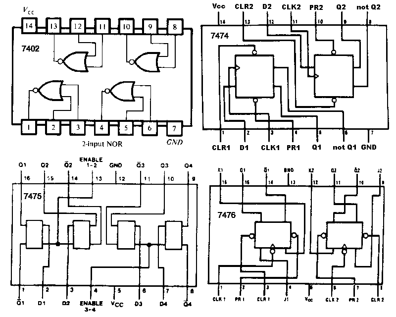
| Figure 1 -- Pin outs for the 7402, 7474, 7475 and 7476 chips. |
Dangerous line voltages are present at the outlets on your work bench. Do not inert anything other than approved power plugs into these outlets.
The voltages and currents produced by the Digi Designer are generally safe. However, you should not short +5V (Vcc) or logic High outputs directly to ground or intentionally make yourself part of a logic circuit.
Chip pins and the tips of the small wires may be sharp. Handle with care. Chips can become very hot if wired incorrectly. Be careful.
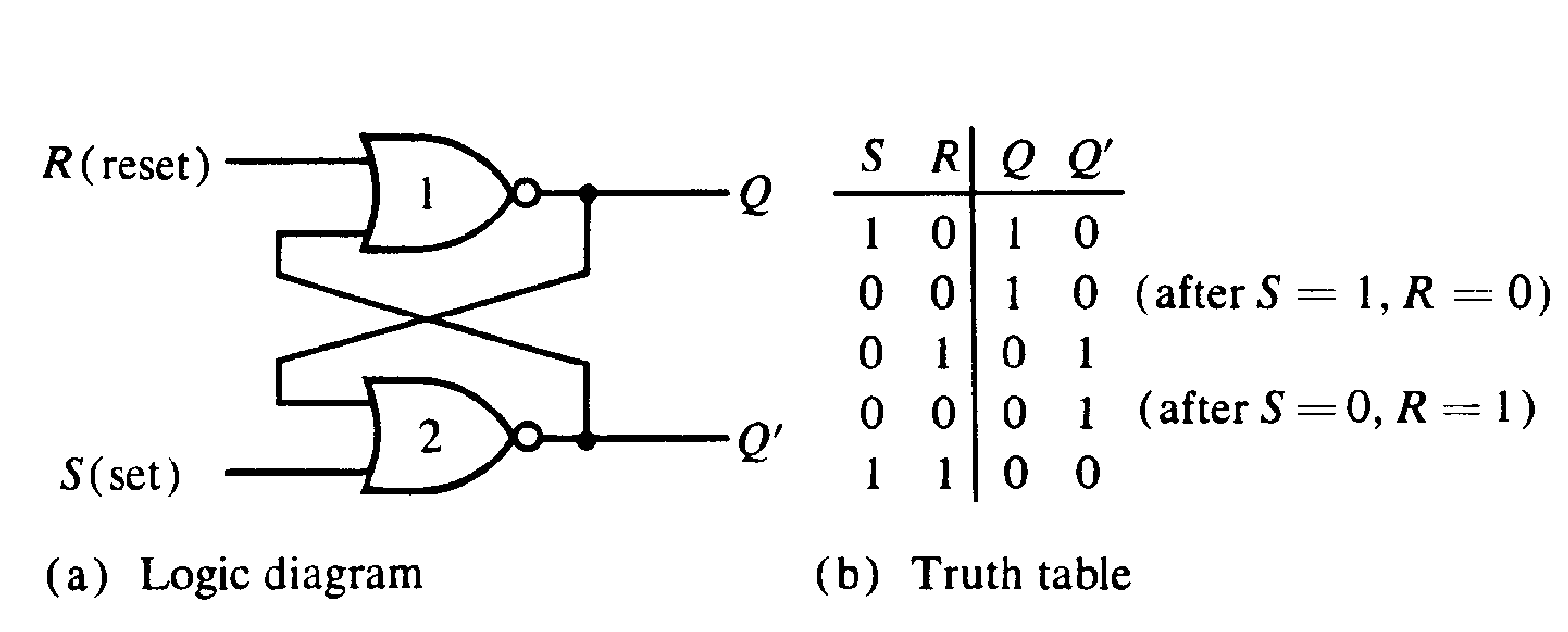 |
| Figure 1 -- An RS flip-flop can be constructed using two NOR gates from a 7402. |
Make the following connections to your chip:
| Pin | Function | Connection |
|---|---|---|
| 1 | Q output | J1, LED |
| 2 | Reset input | J21, normally low pulser |
| 3 | First feedback path | Pin 4, NOT Q output |
| 4 | NOT Q output | J2, LED |
| 5 | Set input | J19, normally low pulser |
| 6 | Second feedback path | Pin 1, Q output |
Confirm that your circuit produces the outputs shown in Figure 2 (b). Does this behavior make sense in terms of the names of the inputs (Set and Reset)?
Disassemble your circuit and remove the 7402 from your Digi Designer.
Insert a 7474 chip into the bread board on your Digi Designer. Connect power and ground to pins 14 and 7, respectively. Make the following connections to your chip:
| Pin | Function | Connection |
|---|---|---|
| 1 | Clear (active low) input | +5 volts, logic high |
| 2 | D input | J19, normally low pulser |
| 3 | Clock input | J13, Digi Designer Clock output |
| 4 | Preset (active low) input | +5 volts, logic high |
| 5 | Q output | J3, LED |
Also connect the Digi Designer clock output to an LED (J1) and the pulser output (D input) to another LED (J2). Set the Digi Designer clock to 1 Hz. The output, Q, of the flip-flop should change to reflect the input, D, only when the clock input goes from low to high. Observer you circuit carefully and confirm it is functioning as expected.
Disassemble your circuit and remove the 7474 from your Digi Designer.
Insert a 7475 chip into the bread board on your Digi Designer. Connect power and ground to pins 5 and 12, respectively (note these are not the standard positions for these connections). Make the following connections to your chip:
| Pin | Function | Connection |
|---|---|---|
| 2 | Data input | J19, normally low pulser |
| 13 | Enable (or gate) input | J21, normally low pulser |
| 16 | Q output | J3, LED |
Also connect pulser J19 (Enable) an LED (J1) and pulser J21 (Data input) to another LED (J2).The output, Q, of the latch should change to reflect the Data input only when the Enable input input is high. Observer you circuit carefully and confirm it is functioning as expected. Compare the behavor of the 7475 to the 7474 you used in the previous circuit.
Disassemble your circuit and remove the 7475 from your Digi Designer.
Insert a 7476 chip into the bread board on your Digi Designer. Connect power and ground to pins 5 and 13, respectively. Make the following connections to your chip:
| Pin | Function | Connection |
|---|---|---|
| 1 | Clock input | J13, Digi Designer Clock output |
| 2 | Preset (active low) input | +5 volts, logic high |
| 3 | Clear (active low) input | +5 volts, logic high |
| 4 | J, input | J19, normally low pulser |
| 15 | Q output | J2, LED |
| 16 | K, input | J21, normally low pulser |
Also connect the Digi Designer clock output to an LED (J1). Set the Digi Designer clock to 1 Hz. The output, Q, of the flip-flop should change in response to the J and K inputs when the clock input goes from low to high. When used alone, the J input sets the flip-flop and the K input clears the flip-flop. When both J and K are high the flip-flop toggles (changes state). Observer you circuit carefully and confirm it is functioning as expected.
Disassemble your circuit and remove the 7476 from your Digi Designer.
Figure 2 was taken from Digital Design, 2nd ed. by M. Morris Mano.